SDRAM Controller FPGA Design
Dec. 2023 - Aug. 2024
Introduction
In this project, I designed and implemented an SDRAM controller for interfacing with an FPGA. The goal was to enable efficient external memory access—handling both read and write operations—while ensuring correct timing and refresh behavior for the SDRAM.
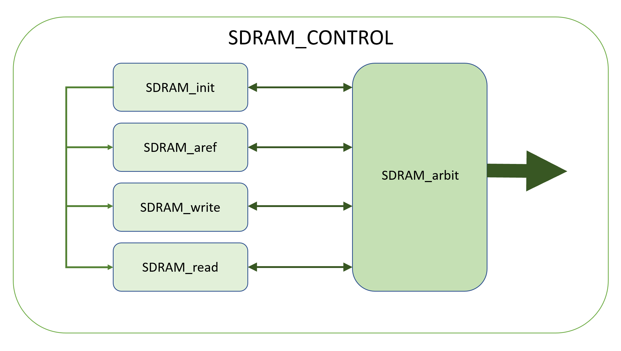
The diagram above shows the high-level architecture of the sdram_ctrl module. It includes several submodules:
sdram_inithandles the initialization sequence required by SDRAM before any operations can take place.sdram_writeandsdram_readmanage the data transfers to and from memory.sdram_arefensures the SDRAM is refreshed periodically to preserve data integrity.sdram_arbitcoordinates the access between the different modules to avoid conflicts and ensure smooth operation.
All of this was implemented in Verilog, and I verified the design through simulation using custom test vectors. This project gave me hands-on experience with memory timing, burst access, and hardware control logic—skills that are crucial in digital system design. Now I will go in depth talk about each module.
Initial Module
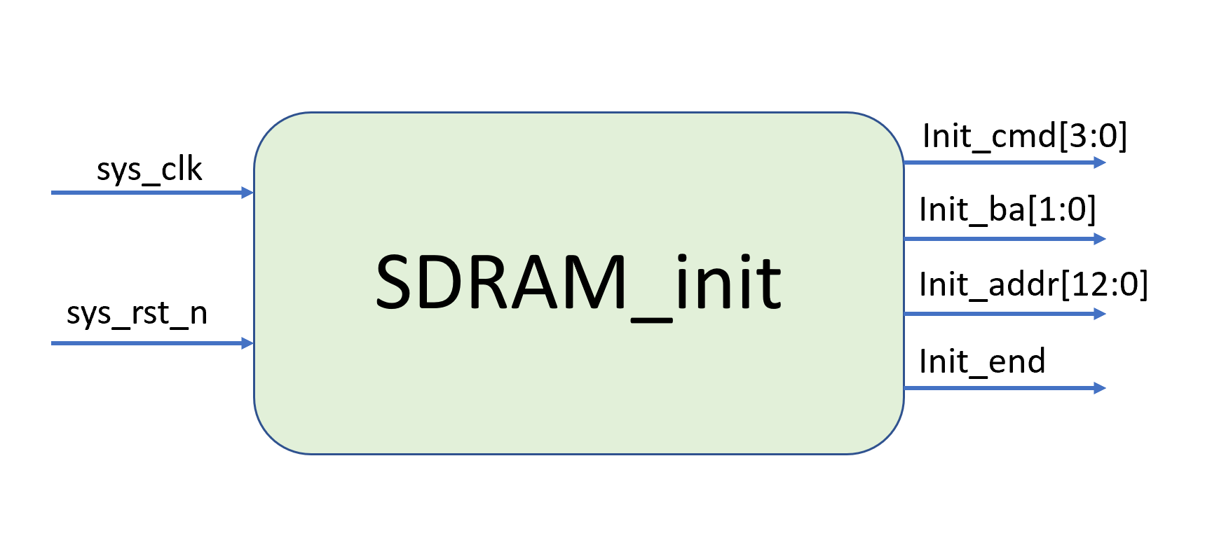
sys_clk: 1-bit input. System clock, frequency 100 MHz.sys_rst_n: 1-bit input. Reset signal, active low.init_cmd: 4-bit output. Command signal output during the initialization phase.init_ba: 2-bit output. L-Bank address used during the initialization phase.init_addr: 13-bit output. Address bus used during initialization to assist with precharge and mode register configuration.init_end: 1-bit output. Flag indicating initialization is complete, allowing SDRAM to proceed with other operations.
The sdram_init module handles the entire power-up and setup sequence required by SDRAM before any read or write operations can happen. SDRAMs aren’t ready to go right after power-on—they require a specific set of commands issued in a strict order with timing delays between them.
Here’s how the module works:
- When the system starts, the controller waits for 200 microseconds to let the SDRAM stabilize.
- It then moves through a sequence of state transitions, each responsible for sending a command:
- Precharge – preps the SDRAM by closing all open rows.
- Auto-refresh – repeated 8 times to refresh internal cells.
- Mode Register Set (MRS) – configures SDRAM settings like CAS latency, burst length, and access type.
- Each state includes built-in wait cycles (e.g., tRP, tRC, tMRD) to satisfy SDRAM timing requirements.
- Once initialization is complete, the
init_endsignal goes high, telling the rest of the system that the SDRAM is ready for normal use.
Key outputs like init_cmd, init_ba, and init_addr are used to drive the SDRAM’s command bus during this sequence. Internally, the module uses counters and flags to track wait times and state transitions.
Pseudocode for Initialization FSM
IF reset is active:
  state ← INIT_IDLE
ELSE:
  SWITCH (state):
CASE INIT_IDLE:
  WAIT for 200us
→ INIT_PRE
    CASE INIT_PRE:
        issue PRECHARGE command
        → INIT_TRP
    CASE INIT_TRP:
        WAIT tRP cycles
        → INIT_AR
    CASE INIT_AR:
        issue AUTO-REFRESH command
        → INIT_TRF
    CASE INIT_TRF:
        WAIT tRC cycles
        IF refresh count == 8:
            → INIT_MRS
        ELSE:
            → INIT_AR
    CASE INIT_MRS:
        issue MODE REGISTER SET command
        → INIT_TMRD
    CASE INIT_TMRD:
        WAIT tMRD cycles
        → INIT_END
    CASE INIT_END:
        assert init_end = 1
        stay here
AutoRefresh Module
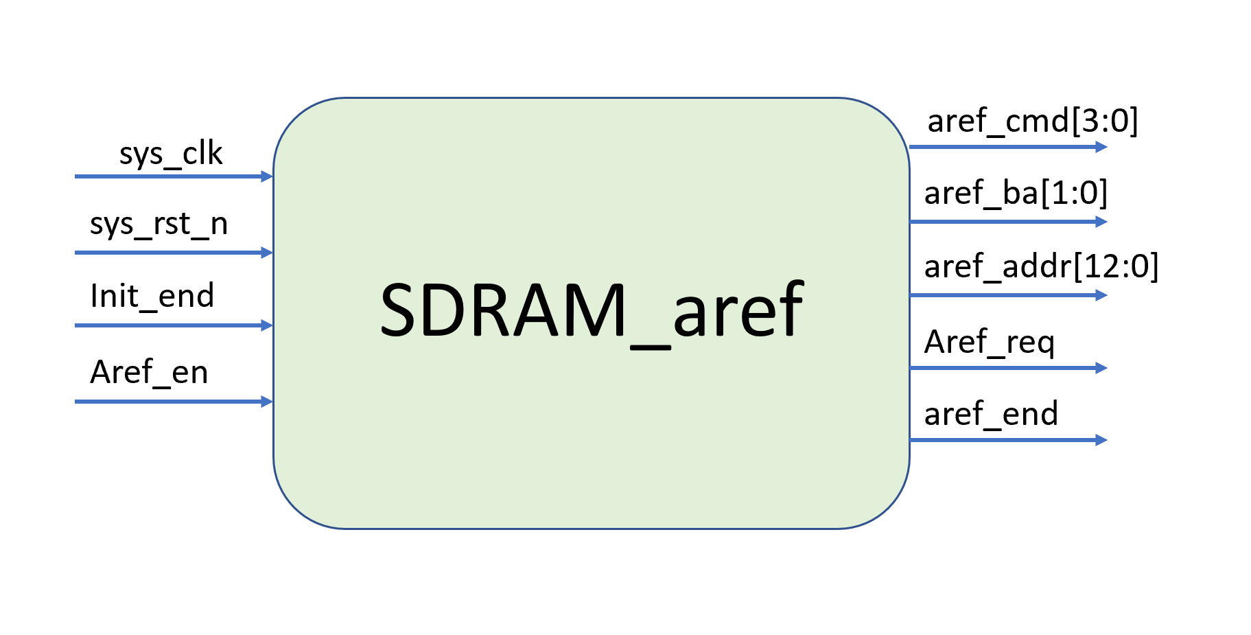
sys_clk: 1-bit input. System clock, frequency 100 MHz.sys_rst_n: 1-bit input. Reset signal, active low.init_end: 1-bit input. Signal indicating initialization is complete.aref_en: 1-bit input. Auto-refresh enable signal.aref_req: 1-bit output. Auto-refresh request signal.aref_cmd: 4-bit output. Auto-refresh phase command signal.aref_ba: 2-bit output. L-Bank address for auto-refresh phase.aref_addr: 13-bit output. Address bus for auto-refresh phase.aref_end: 1-bit output. Signal indicating end of auto-refresh phase.
How it work?
- After initialization (
init_end), the module waits for 7.5 µs (CNT_REF_MAX) before sending a refresh request. - When the time is up, it raises
aref_reqto start a refresh. - The module then goes through a small FSM (finite state machine):
States:
AREF_IDLE: Waits for refresh to be enabled.AREF_PCHA: Issues a precharge command.AREF_TRP: WaitstRPcycles after precharge.AUTO_REF: Sends the auto-refresh command.AREF_TRF: WaitstRCcycles after refresh.AREF_END: Refresh complete → back to IDLE.
Pseudocode for AutoRefresh
On power-up:
    Wait until init_end and aref_en are both high

Every 7.5 µs (based on cnt_aref):
    Trigger aref_req to start refresh

Refresh Sequence:
    → Precharge             // closes any open rows before refresh
    → Wait tRP cycles       // tRP = Row Precharge time (minimum delay before next command)

    → Auto-Refresh command  // triggers internal SDRAM refresh
    → Wait tRC cycles       // tRC = Row Cycle time (minimum time between refresh commands)

    → Repeat Auto-Refresh (total 2 times per cycle)
    → Set aref_end = 1      // marks end of the refresh operation
Write Module
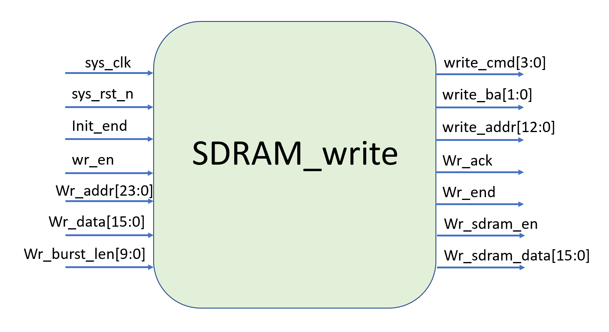
sys_clk: 1-bit input. System clock, frequency 100 MHz.sys_rst_n: 1-bit input. Reset signal, active low.init_end: 1-bit input. Signal indicating initialization is complete.wr_en: 1-bit input. Write enable signal for data.wr_addr: 24-bit input. Address input for data write stage.wr_data: 16-bit input. Data input for data write stage.wr_burst_len: 10-bit input. Burst length for write operation.wr_ack: 1-bit output. Acknowledge signal for write operation.wr_end: 1-bit output. Signal indicating end of a single write burst.write_cmd: 4-bit output. Command signal for data write stage.write_ba: 2-bit output. Logical bank address for data write stage.write_addr: 13-bit output. Address output for data write stage.wr_sdram_en: 1-bit output. SDRAM output enable for data write stage.wr_sdram_data: 16-bit output. SDRAM data output for data write stage.
This module handles writing data from the FPGA to SDRAM in burst mode. It's triggered when wr_en is asserted and init_end confirms the SDRAM is ready.
The module walks through a finite state machine that performs all necessary steps for a safe and valid SDRAM write transaction, including activation, writing, and precharge.
FSM Main States:
WR_IDLE → Wait for write enable (wr_en) and init_end
WR_ACTIVE → Activate the target row (ACTIVE command)
WR_TRCD → Wait tRCD (row-to-column delay)
WR_WRITE → Issue WRITE command to begin burst write
WR_DATA → Output actual data for N clock cycles
WR_PRE → Issue PRECHARGE command to close the row
WR_TRP → Wait tRP (precharge time)
WR_END → Write complete, go back to IDLE
Outputs:
write_cmd: Command sent to SDRAM (ACTIVE, WRITE, P_CHARGE, etc.)
write_ba: Bank address of the SDRAM
write_addr: Row/column address (derived from wr_addr)
wr_ack: Indicates write is acknowledged (ready to send data)
wr_end: Pulse that signals the burst write has finished
wr_sdram_en: Enables SDRAM data output
wr_sdram_data: The data being sent to SDRAM (driven by wr_data)
Pseudocode for Write
IF reset:
    state ← WR_IDLE

FSM:
    WR_IDLE:
        IF wr_en && init_end → WR_ACTIVE

    WR_ACTIVE:
        Send ACTIVE command
        → WR_TRCD

    WR_TRCD:
        Wait tRCD cycles
        → WR_WRITE

    WR_WRITE:
        Send WRITE command
        → WR_DATA

    WR_DATA:
        FOR wr_burst_len cycles:
            Output wr_data to SDRAM
        After burst ends → WR_PRE

    WR_PRE:
        Send PRECHARGE command
        → WR_TRP

    WR_TRP:
        Wait tRP cycles
        → WR_END

    WR_END:
        → Return to WR_IDLE
Read Module
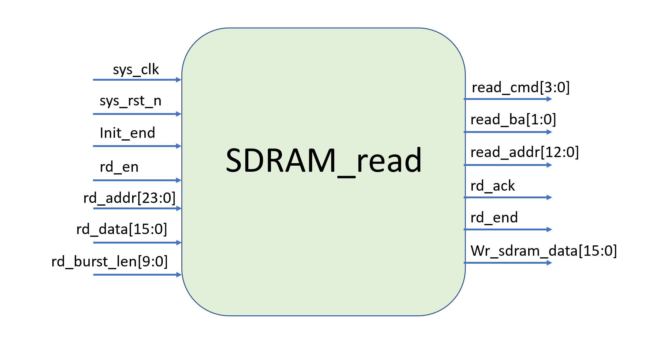
sys_clk: 1-bit input. System clock, frequency 100 MHz.sys_rst_n: 1-bit input. Reset signal, active low.init_end: 1-bit input. Signal indicating initialization is complete.rd_en: 1-bit input. Data read enable signal.rd_addr: 24-bit input. Address input for the data read stage.rd_data: 16-bit input. Data input for the read stage (usually from FIFO or intermediate logic).rd_burst_len: 10-bit input. Burst length for the read operation.rd_ack: 1-bit output. Acknowledge signal for read operation.rd_end: 1-bit output. Signal indicating end of a burst read.read_cmd: 4-bit output. Command signal during data read stage.read_ba: 2-bit output. Logical L-Bank address during data read stage.read_addr: 13-bit output. Address output for data read stage.rd_sdram_data: 16-bit output. Data output from SDRAM during the read phase.
This module manages burst read operations from SDRAM. It waits until the SDRAM is initialized, then responds to a read enable (rd_en) signal, fetches data from SDRAM, and outputs it via rd_sdram_data.
FSM Flow:
RD_IDLE → Wait for rd_en + init_end
RD_ACTIVE → Send ACTIVE command to open the row
RD_TRCD → Wait tRCD (Row to Column Delay)
RD_READ → Issue READ command
RD_CL → Wait tCL (CAS Latency)
RD_DATA → Read data out for rd_burst_len cycles
RD_PRE → Issue PRECHARGE command to close the row
RD_TRP → Wait tRP (Precharge time)
RD_END → Done; return to IDLE
Pseudocode for Read
IF reset:
    state ← RD_IDLE

FSM:
    RD_IDLE:
        IF rd_en AND init_end → RD_ACTIVE

    RD_ACTIVE:
        Send ACTIVE command to select row
        → RD_TRCD

    RD_TRCD:
        Wait tRCD cycles
        → RD_READ

    RD_READ:
        Send READ command
        → RD_CL

    RD_CL:
        Wait tCL cycles (CAS Latency)
        → RD_DATA

    RD_DATA:
        Output rd_data to rd_sdram_data
        FOR rd_burst_len cycles
        → RD_PRE

    RD_PRE:
        Send PRECHARGE to close row
        → RD_TRP

    RD_TRP:
        Wait tRP
        → RD_END

    RD_END:
        → Return to RD_IDLE
Arbit Module
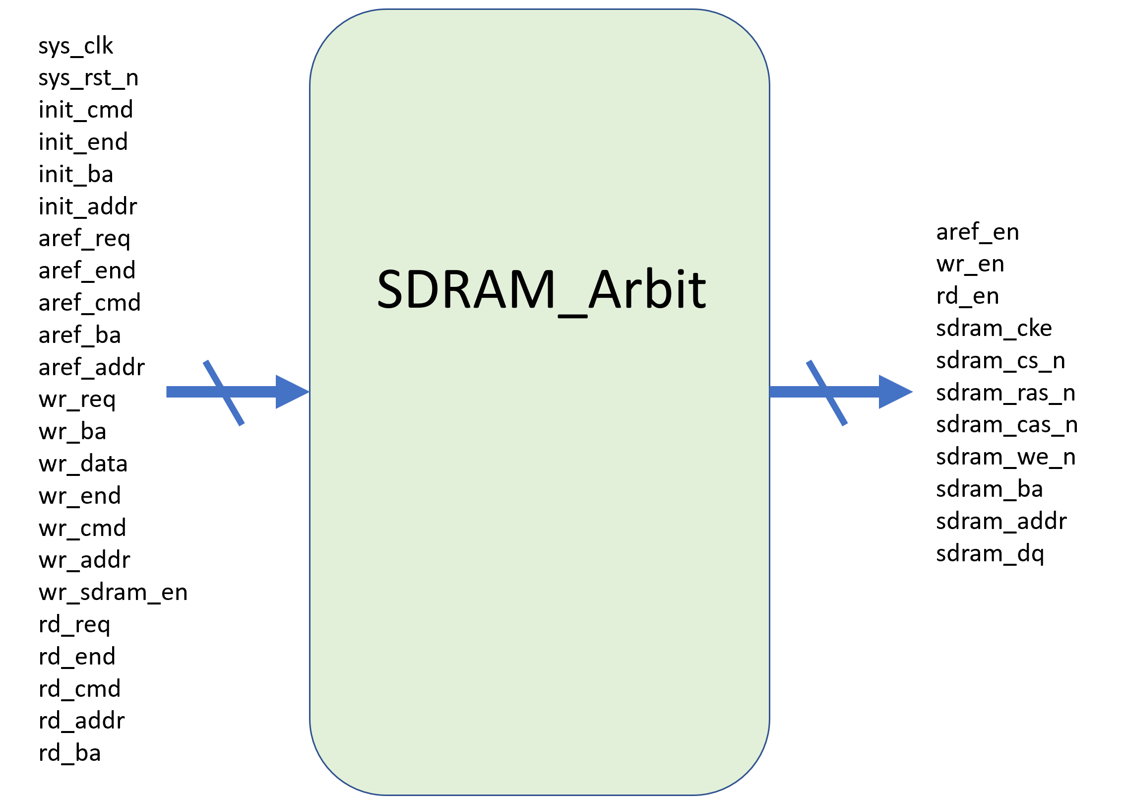
| Signal | Width | Direction | Description |
|---|---|---|---|
| sys_clk | 1 Bit | Input | System clock, 100 MHz |
| sys_rst_n | 1 Bit | Input | Reset signal, active low |
| init_cmd | 4 Bit | Input | Initialization command |
| init_ba | 2 Bit | Input | Bank address during initialization |
| init_addr | 13 Bit | Input | Address bus during initialization |
| init_end | 1 Bit | Input | Initialization complete signal |
| aref_req | 1 Bit | Input | Auto-refresh request signal |
| aref_cmd | 4 Bit | Input | Auto-refresh command |
| aref_ba | 2 Bit | Input | Bank address during auto-refresh |
| aref_addr | 13 Bit | Input | Address bus during auto-refresh |
| aref_end | 1 Bit | Input | Auto-refresh complete signal |
| wr_req | 1 Bit | Input | Write request signal |
| wr_cmd | 4 Bit | Input | Write command |
| wr_ba | 2 Bit | Input | Write bank address |
| wr_addr | 13 Bit | Input | Write address bus |
| wr_sdram_en | 1 Bit | Input | SDRAM data output enable (for write) |
| wr_data | 16 Bit | Input | Data to write to SDRAM |
| wr_end | 1 Bit | Input | Write burst complete signal |
| rd_req | 1 Bit | Input | Read request signal |
| rd_cmd | 4 Bit | Input | Read command |
| rd_ba | 2 Bit | Input | Read bank address |
| rd_addr | 13 Bit | Input | Read address bus |
| rd_end | 1 Bit | Input | Read burst complete signal |
| aref_en | 1 Bit | Output | Auto-refresh enable |
| wr_en | 1 Bit | Output | Write enable |
| rd_en | 1 Bit | Output | Read enable |
| sdram_cke | 1 Bit | Output | SDRAM clock enable |
| sdram_cs_n | 1 Bit | Output | SDRAM chip select (active low) |
| sdram_cas_n | 1 Bit | Output | SDRAM column address strobe (active low) |
| sdram_ras_n | 1 Bit | Output | SDRAM row address strobe (active low) |
| sdram_we_n | 1 Bit | Output | SDRAM write enable (active low) |
| sdram_ba | 2 Bit | Output | SDRAM bank address |
| sdram_addr | 13 Bit | Output | SDRAM address bus |
| sdram_dq | 16 Bit | Output | SDRAM data bus |
This is the arbiter module that controls access to the SDRAM by coordinating which module (initialization, refresh, write, or read) can drive the SDRAM command/address/data lines at any moment. Only one can access it at a time.
It implements a priority-based FSM to decide who gets access to the SDRAM:
Priority order:
- Initialization
- Auto-refresh
- Write
- Read
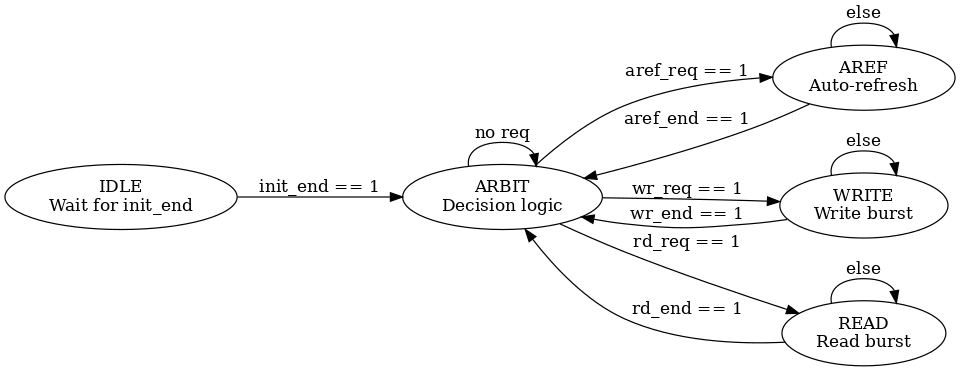
| State | Meaning |
|---|---|
| IDLE | Waiting for initialization to finish |
| ARBIT | Arbitration decision state |
| AREF | Handles auto-refresh |
| WRITE | Handles write burst |
| READ | Handles read burst |
Initial State:
    If init_end == 0 → Stay in IDLE
    If init_end == 1 → Go to ARBIT

ARBITRATION:
    If aref_req → AREF
    Else if wr_req → WRITE
    Else if rd_req → READ
    Else → Stay in ARBIT

AREF:
    If aref_end → Return to ARBIT

WRITE:
    If wr_end → Return to ARBIT

READ:
    If rd_end → Return to ARBIT

Always drive SDRAM outputs with:
    - current state’s command (init_cmd / aref_cmd / wr_cmd / rd_cmd)
    - bank address and row/col address
This module ensures conflict-free SDRAM access. For example:
- You don't want a write to interrupt an auto-refresh.
- You don't want both read and write trying to drive
sdram_dq.
It simplifies the system by putting access control logic in one place and makes sure the SDRAM always receives valid timing-respecting commands.
Conclusion
Through this project, I successfully designed and implemented a fully functional SDRAM controller capable of handling initialization, auto-refresh, read, and write operations on an FPGA platform. By breaking down the controller into modular components—such as sdram_init, sdram_a_ref, sdram_write, sdram_read, and sdram_arbit—I was able to manage complex timing and command sequences required by SDRAM protocols.